ULTRA-LOW DISTORTION, EMI/RFI HARDENED, ACTIVE 2-CH BUFFER / 3-WAY SPLITTER FRONT END FOR AMPLIFIER BUILDERS
INTRODUCTION
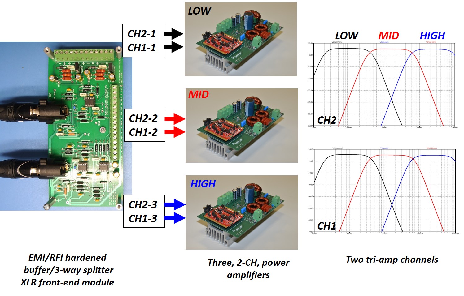
Described here is a 2-channel stand-alone amplifier front end module that accepts a small signal input from a typical 600 Ohm source impedance and splits it into three, non-inverted, independent and (essentially) identical single-ended output signals, each capable of driving an amplifier, active filter or meter amplifier. The module can be used as a splitter for a 3-way, tri-amplified loudspeaker system where each signal is sent to a dedicated amplifier sized for low, mid and high frequency drivers. The figure below illustrates the idea. Passive nets for low, mid and high frequencies are used to provide large signal filtering after the amplifier outputs. Although the figure shows CL-D "chip" type amplifiers, audio amplifiers of any type will work. Note also the power supplies for the components are not shown.
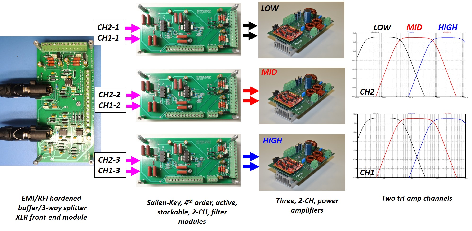
An alternative filtering scheme to the above and preferred approach is to employ active filters between the buffered signals and associated amplifiers. That concept is shown below and, as before, three amplifiers are used and sized for the low, mid and high frequency drivers in the system. Note that North Reading Engineering has designed low distortion Sallen-Key evaluation module that is ideally suited for providing builders and engineers the active filtering in this setup.
With the addition of level controls (i.e. attenuator pads) the module can also be used as an ultra-low distortion preamplifier or, by increasing the gain of the op-amps, a super quiet headphone amp.
TECHNICAL DESCRIPTION
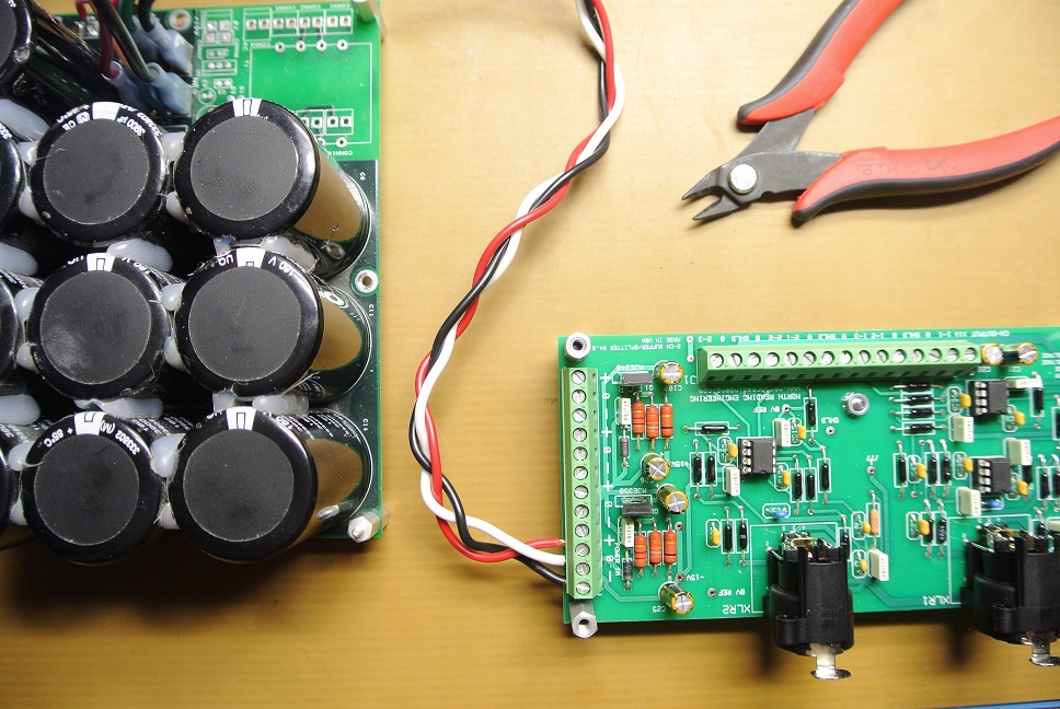
The module can provide any audio amplifier with a quiet, ultra-low distortion, 2-channel XLR/TRS front end. XLR combo connectors have been selected to provide both balanced XLR/TRS inputs or, using adapters, un-balanced RCA inputs. Input voltage and small signal output connections are made using Phoenix Contact, screw clamp, terminal blocks. Boards are fabricated in the USA. Pb-free, RoHS compliant assemblies are also available.
Op-amp packages are installed in Mill-Max sockets which allows for replacement of damaged devices or substitutions (the LME49720 may be EOL in 2018). The LME5532 for example, is an excellent alternative package for driving low impedance loads (most audio amplifier inputs have input impedances that exceed 10k Ohms).
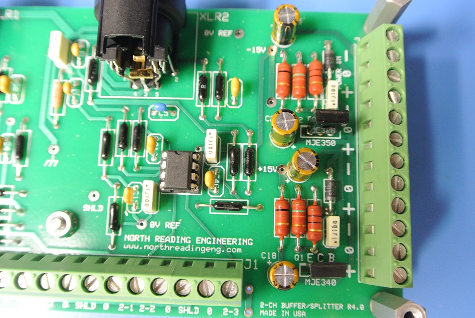
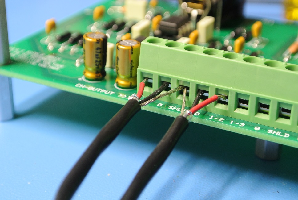
Below are photos of the module. Top right shows the terminal block used to make the output connections from the module to the drive devices. This terminal block is labeled J1.
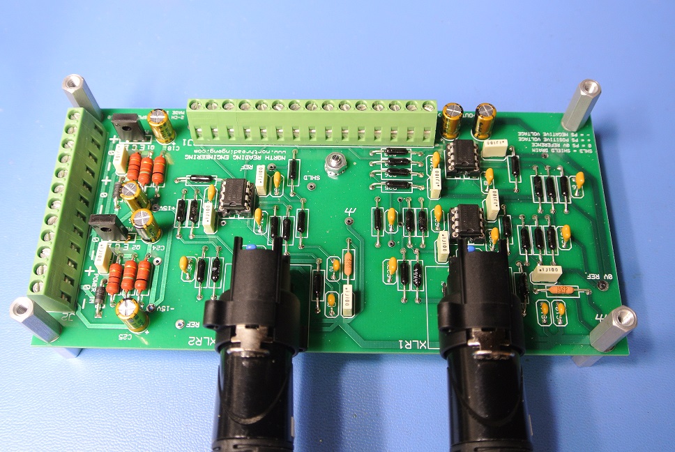
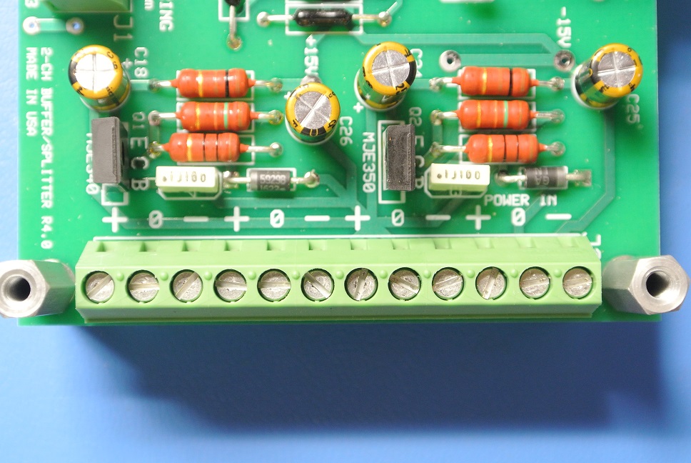
Bottom left, the +/-15VDC, on-board power supply is shown adjacent to the input voltage terminal block labeled J2. Top view of terminal block J2 is shown lower right.
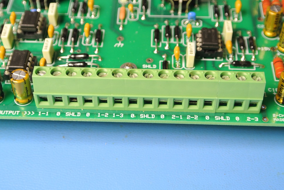
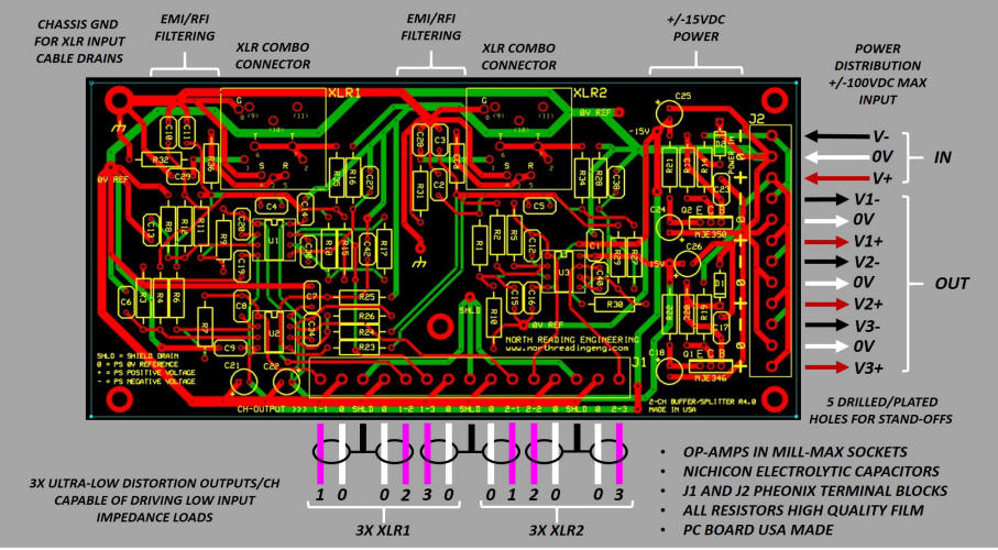
All possible connections to the module are shown in the image below. External power supply voltage is provided at the POWER IN connections of J2. To facilitate the distribution of power to other small signal circuits, J2 provides voltage taps for three additional circuits (total current drawn not to exceed 3A). Buffered and split outputs are shown at J1.
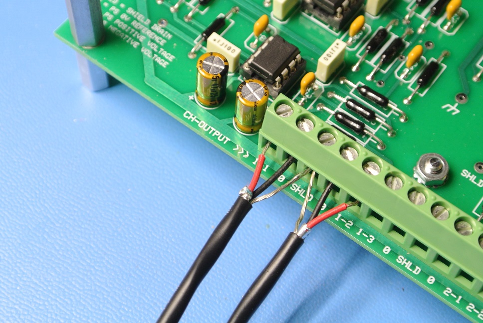
Typical small signal outputs made at J1 are shown below using two-lead, shielded wire (Alpha Wire, 2461C). Each output consists of the signal lead (RED), 0V power supply reference (BLK) and shield drain (bare). Note that a pair of adjacent cable drains share a common terminal connection. All shield drains trace back to a common solder pad that can be wired to chassis GND. The terminal blocks provide excellent clamp-down force on the lead wires. Connections will not loosen from vibration.
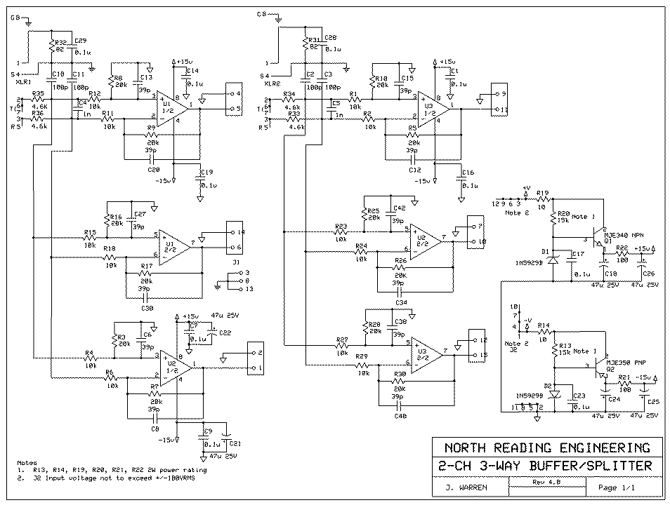
The schematic for the design is shown below. The front end of each channel is configured with a general purpose, common mode/differential mode EMI/RFI filter useful in environments with high levels of environmental noise. Looking at the XLR1 front end (the XLR2 front end and layout is identical), the complimentary RC pairs R35, C10 and R36, C11 provide common mode input rail filtering whilst R35, R36 and C4 provide differential mode filtering. Circuit common mode rejection (CMR) depends on the time constants of the complimentary RC pairs be matched otherwise reductions in CMR are realized. The front end design requires precisely matched resistors. All metal film resistor values are matched to better that +/-0.05% tolerance from +/-1.0% lots. Resistor temperature coefficients of 15PPM/°C are standard.
Using the feedback scheme shown in the schematic, bandwidth measurements with LME49720 dual op-amp package evidences a -3dB frequency at 37kHz. The measurement is made with each output at a load of 10k Ohm. Input impedance is 16k Ohms measured with a balanced input source impedance of 660 Ohm. Differential attenuation of the buffer circuit is about 1.0dB.
Capacitor C4 reduces differential EMI/RFI signals on the inputs. Differential mode -3dB frequency is about 60kHz. Both C10, C11, XLR shield (Pin 1) and the XLR connector body shunt to chassis ground. Cable shield drain wire from Pin 1 sinks to chassis ground through a hybrid, parallel RC filter. The chassis ground connection is identified on the board and is independent of the small signal 0V power supply reference. The on-board, regulated +/-15VDC supply (unloaded) provides power to the three, dual op-amp packages. The on-board supply requires an external power supply capable of providing between +/-18 to +/-100VDC. Although a dedicated power supply can be used to drive the board, taps from the output stage rails of the amplifier supply can also be used. MJE340G/350G, 0.5A complementary power transistors in TO-225 packages are used in the supplies.
PERFORMANCE PLOTS
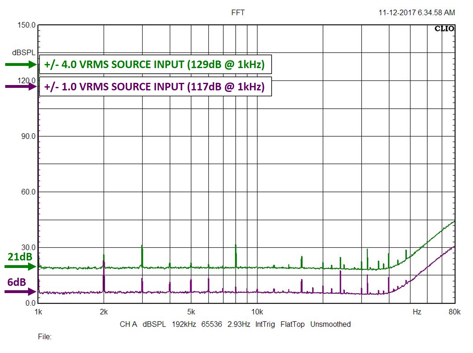
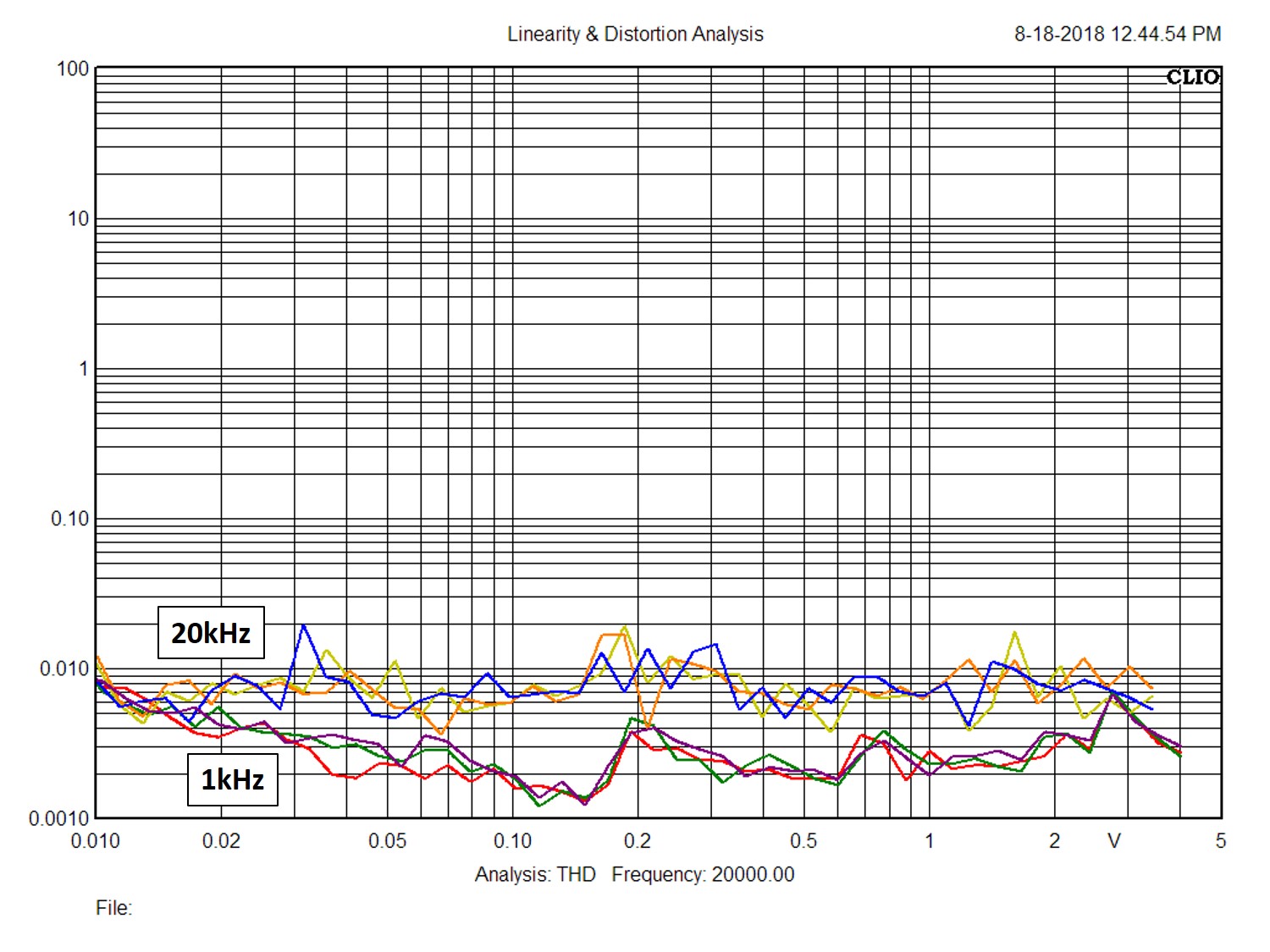
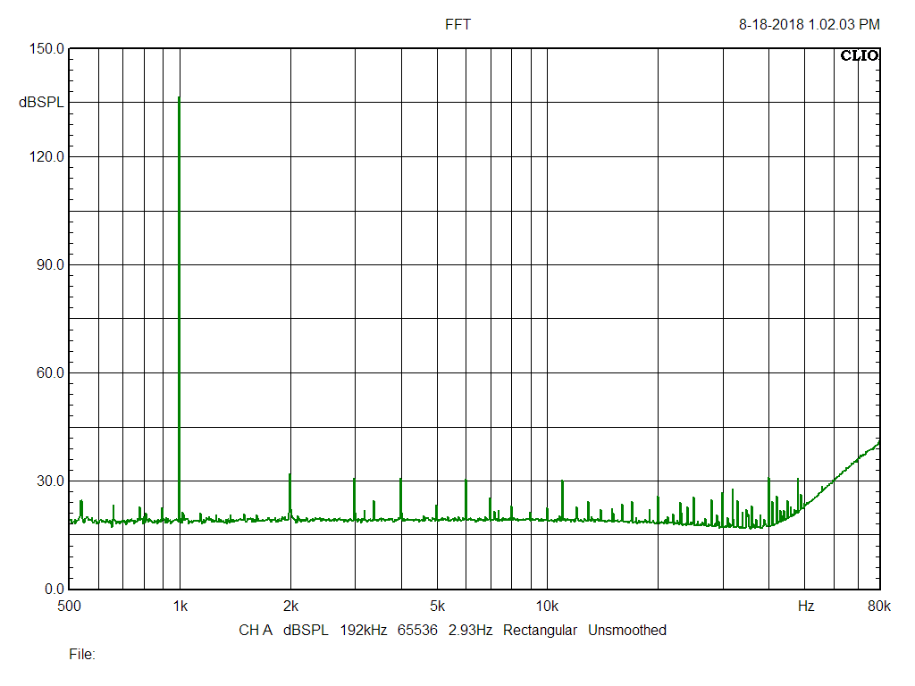
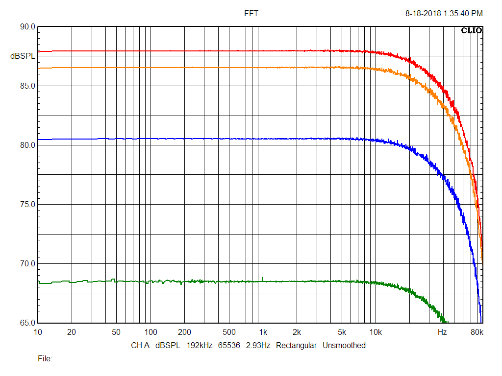
Fast Fourier Transform (FFT) of buffered output at two input levels, all outputs at RL=10k Ohm, balanced input. FFT at 192kHz sampling rate, flat-top windowing. Small differences in harmonic content is shown but overall, %THD is very low as is evidenced in the second plot showing %THD from 10mV to 4VRMS module output at two test frequencies, 1kHz and 20kHz. Three runs at each frequency are shown.
BALANCED INPUTS
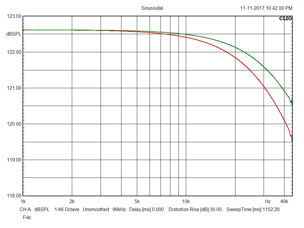
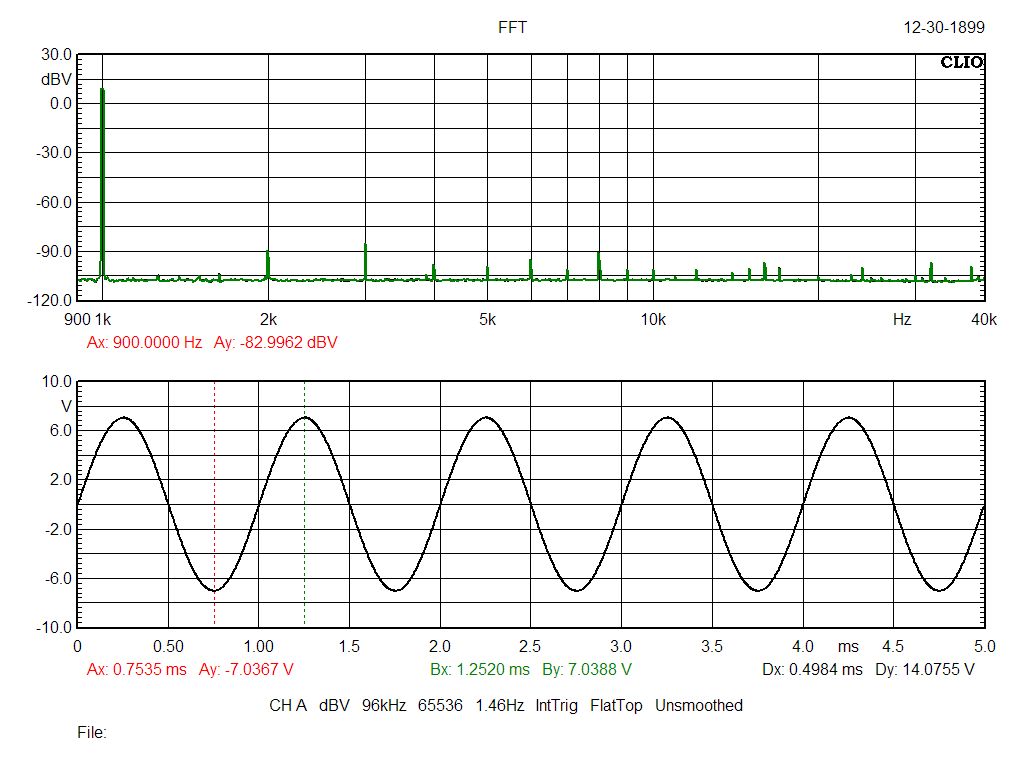
Bandwidth from 1kHz to just over 40kHz of both the buffer output (red) measured at the output terminal and differential mode filter (green) are shown below. To make the bandwidth comparison easier to interpret, the differential mode bandwidth plot was shifted "up" in dB to coincide with the buffered output plot at 1kHz. With the input filtering shown in the schematic, the 20kHz, -3db frequency of the buffered output and differential mode filter are -1.6 and -1.0dB relative to the input signal, respectively. As shown below, a +/-7.0Vp-p output swing with balanced, 1kHz input evidences very low harmonic content to 40kHz (0.003%THD).
UNBALANCED INPUTS
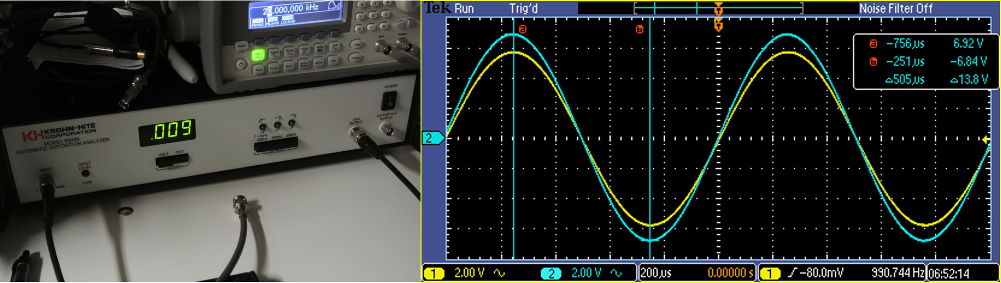
Shown below are scope traces of an unbalanced, 1kHz test signal from the internal calibration generator of the Krohn-Hite 6900B distortion analyzer being used to measure %THD at the buffer output. The source impedance of the analyzer is 600 Ohms and the no-load voltage is 14.2Vp-p or 5.0Vrms. The blue trace is the generator output voltage loaded with the buffer, measured between the XLR1 connector Pin 2 (13.8Vp-p or 4.9Vrms) and circuit ground reference. The buffer output (yellow trace) is with a 560 Ohm load across the op-amp output pin (11.5Vp-p or 4.1Vrms). Using this data, buffer unbalanced input impedance is calculated to be 16kOhm. Distortion is 0.009% THD, all analyzer filters out. Note the 6900B is capable of measuring distortion components to 1MHz.
COMMON MODE REJECTION
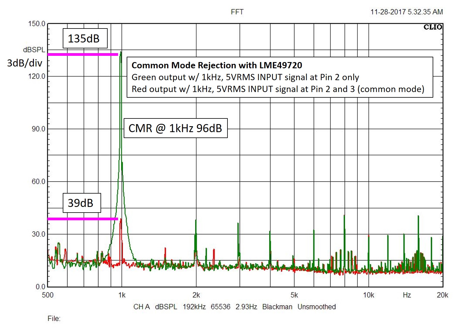
The red plot below is the FFT response at the output of one channel with a 5VRMS amplitude, 1kHz sine wave input signal (0.002%THD) applied to both the inverting (Pin 2) and non-inverting (Pin 3) inputs. The green FFT is the output of the same channel with the input signal applied to the non-inverting input (Pin 2 alone). As shown, the common mode rejection of the circuit at the 1kHz input signal is >90dB. For the module under test, the resistor pairs were selected to be within +/-0.02% or better of the nominal values shown in the schematic. Note that the test setup used here, the input signal and the sampling clock of the analyzer are not synchronized so and a Blackman window was used to provide side lobe attenuation so some spectral leakage.
The module is exceedingly quiet and makes for an excellent HiFi preamplifier.
POWER SUPPLYS
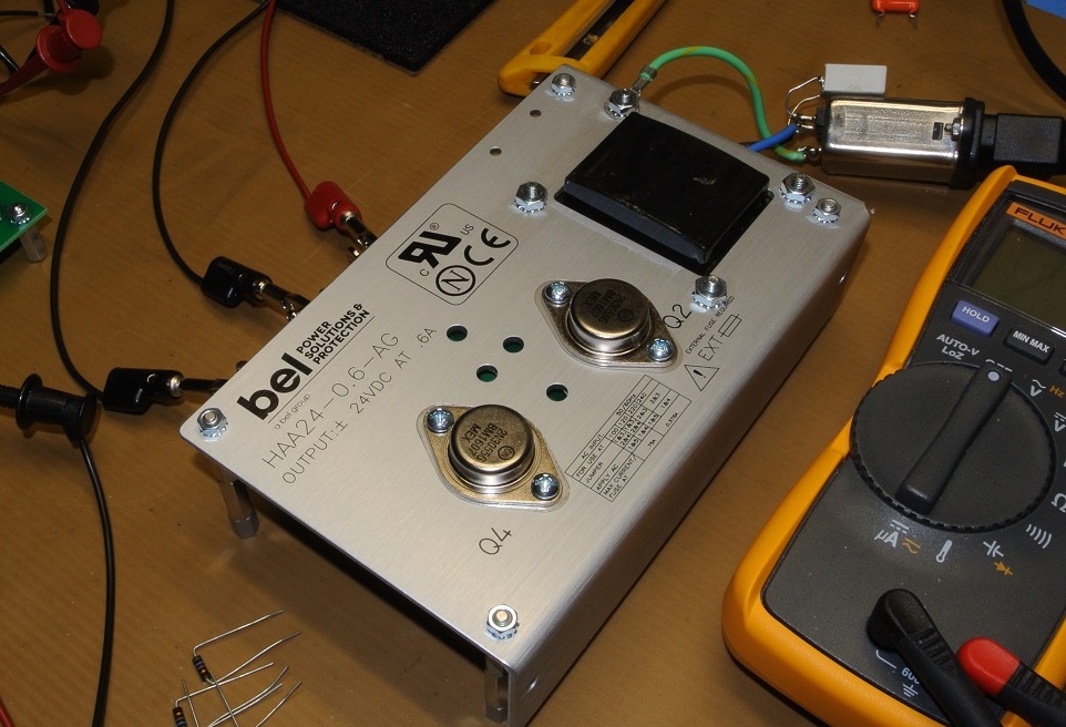
For builders that intend to use the module as a stand-alone preamplifier or buffer stage for active filtering, an independent power supply is required. All tests and performance plots shown above were done with a Bel Power Solutions HAA24-0.6-AG, isolated, linear +/-24VDC, 0.6A power supply driving the on-board +/-15VDC supply. The Bel unit is an excellent, relatively low cost (~$70) supply cable of providing power to multiple buffer/splitter modules and active filters. User must install a fuse holder on the power plug.
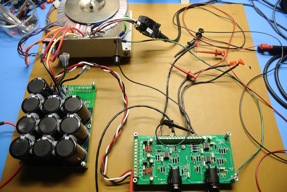
Alternatively, the board can be powered from a conventional center-tap, spilt rail amplifier power supply. Shown below is a +/-100VDC supply with dedicated taps for the buffer board. The supply consists of a toroidal transformer with center-tapped secondary feeding a bridge rectifier and a 40,000uF bank of filter capacitors. Three power supply leads are shown (+V = RED, 0V = REF, -V = BLK) and connected to the corresponding power supply input terminals of J2. With a +/-100VDC supply, the MJE350/340 power transistors reach a steady state temperature of just under 140°C (max. specified 150°C) without heat sinking. Resistors in the on-board supply are all 2W ratings. With modifications to the on-board supply, supply voltages in excess of +/-100VDC can be used (inquire).
FFT of CH1 output with +/-100VDC center-tap, split rail supply. RL=560 Ohm. Output is 5VRMS at 1kHz using balanced input signal. Approximately 105dB of undistorted signal is shown. Second plot shows bandwidth at 0.5, 2.0, 4.0 and 5.0VRMS output.
SUMMARY
If you have interest in either purchasing or building the R4.0 module please contact North Reading Engineering. If you have an application in mind and would like to discuss if the module will work in that application, just send an email (below) and I'll be glad to discuss the application with you.
PRICING
1. Assembled R4.0 Amplifier Module, Aluminum standoffs, performance data: $199
2. R4.0 Kit includes one PC Board, Phoenix Contact Terminal Blocks, Neutrik NCJ6FAH XLR Combination Female Connectors, Mill-max 8-Pin Sockets, LME49720 Dual High Performance, High Fidelity Op-Amps, NPN/PNP Complementary pair MJE350G/340G Power Supply Transistors, Aluminum standoffs and parts list: $99
3. R4.0 PC Board (made in USA), Aluminum standoffs and parts list: $49
This webpage and its contents are the property of John Warren of North Reading Engineering, North Reading, MA 01864 USA. No part of the above work may be copied and published, in part or in total, without written permission.
© 2018 John Warren